
Ireland’s semiconductor industry has evolved into one of Europe’s most strategically important technology hubs. With a strong presence of global manufacturers, a rapidly expanding R&D base, and deep expertise in materials science, the country is increasingly positioned at the intersection of advanced device engineering and next-generation electronics.
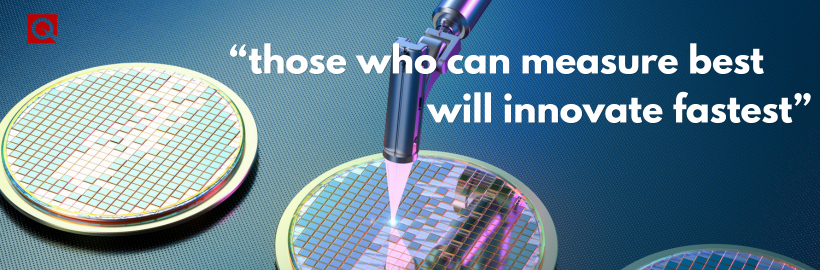
As device architectures move beyond traditional silicon scaling, the challenge is no longer simply fabrication—but understanding behaviour at the nanoscale. In this shift, advanced characterisation tools are becoming essential infrastructure for semiconductor innovation. Within Ireland’s research and industrial ecosystem, the QD-UKI instrumentation portfolio is playing a quietly enabling this transition, supporting work from fundamental materials science through to device-level validation.

Beyond Moore’s Law: Materials-Driven Device Innovation
The semiconductor industry is now firmly in the era of heterogeneous integration—where 2D materials, nanowires, and complex multilayer stacks are replacing conventional bulk silicon scaling.
In Ireland, this shift is visible across both academic and industrial research environments, where new materials are being explored for next-generation logic, photonics, and sensing applications. Facilities working on these challenges increasingly rely on a combination of optical, structural, and electrical characterisation to understand how atomic-scale variations translate into device behaviour.
Spectroscopic ellipsometry systems are widely used to extract thin-film optical constants in emerging semiconductor stacks, including oxides, nitrides, and 2D materials. These measurements are critical for understanding layer thickness, uniformity, and band-structure-related properties in ultra-thin devices.
At the structural level, electron diffraction techniques provide high-resolution insight into crystallography, strain distribution, and defects in nanowires and heterostructures. This capability is particularly important for strain-engineered devices, where even subtle lattice distortions can significantly alter electronic performance.
Together, these tools help bridge the gap between material synthesis and device function, an increasingly important step in Ireland’s expanding semiconductor R&D landscape.
The Measurement Challenge at the Nanoscale
As devices shrink into the nanometre regime, electrical characterisation becomes one of the most significant bottlenecks in semiconductor development. Low-dimensional systems such as organic semiconductors, nanowires, and 2D materials often exhibit signals that sit close to—or within—the noise floor of conventional instrumentation.
To address this, researchers in Ireland and beyond rely heavily on cryogenic and precision transport systems such as those developed by Lake Shore Cryotronics and integrated platforms like those from Quantum Design, including PPMS and VersaLab systems.
These platforms enable:
- Low-temperature transport measurements
- Hall effect and magnetotransport studies
- High-stability I–V characterisation under controlled environments
By reducing thermal noise and improving environmental stability, they allow researchers to isolate intrinsic material behaviour from measurement artefacts—an essential requirement when studying quantum transport, charge trapping, or nonlinear conduction effects.
In Ireland’s semiconductor research ecosystem, these capabilities are increasingly central to work at institutes such as Tyndall National Institute and collaborative industry–academic programmes focused on advanced device physics.
Interconnect Scaling and the Rise of 3D Semiconductor Architectures
While transistor scaling continues to dominate headlines, interconnects are becoming a critical performance limiter in advanced circuits. As copper features shrink, issues such as electromigration, resistivity increase, and thermal instability become more pronounced.
Understanding these effects requires a multi-modal approach to characterisation.
X-ray and spectroscopic systems from providers such as Sigray enable detailed analysis of composition, oxidation states, and buried interface structures within advanced semiconductor stacks. These insights are essential for evaluating reliability in densely packed 3D architectures.
Thermal and optical profiling systems from InfraTec provide complementary information on heat distribution and failure mechanisms, particularly in high-current interconnect structures.
Additionally, high-resolution surface metrology tools such as those from 4D Technology allow precise mapping of surface topography and deformation in complex device geometries.
Together, these tools support a more complete understanding of how electrical, thermal, and mechanical effects interact in modern semiconductor interconnects—a key area of focus as Ireland strengthens its position in advanced manufacturing and packaging technologies.
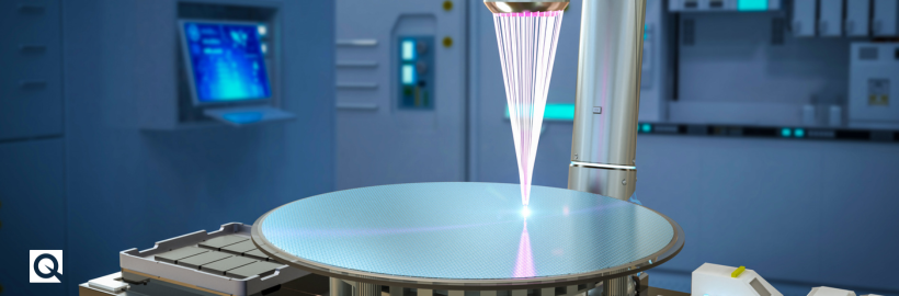
Correlative and Synchronous Measurement: Linking Structure, Transport, and Function
A defining trend in next-generation semiconductor research is the move toward correlative measurement—where structural, electrical, and thermal data are captured in a unified framework rather than isolated experiments.
Platforms such as the correlative microscopy systems developed by Quantum Design enable researchers to align optical, electrical, and structural information within a single experimental environment. This is particularly valuable when studying devices where performance is governed by local variations in strain, defects, or composition.
Similarly, lock-in-based thermal and electrical measurement approaches, including those integrated into advanced testing systems, allow weak signals to be extracted with high precision even in noisy environments.
In practical terms, this means researchers can directly correlate:
- Strain fields (measured via electron diffraction)
- Electrical transport behaviour (measured via cryogenic systems)
- Thermal response (measured via infrared imaging)
This level of correlation is becoming essential for understanding device variability in nanoscale systems, particularly in emerging semiconductor platforms under development across Ireland’s research institutions.
Ireland’s Semiconductor Ecosystem: From Materials to Systems

Ireland’s semiconductor sector is uniquely positioned at the intersection of manufacturing, research, and advanced materials science. With major global fabs, a strong pipeline of engineering talent, and world-class research institutions, the country is increasingly focused on higher-value activities such as device innovation, materials engineering, and advanced characterisation.
Within this ecosystem, the availability of integrated instrumentation portfolios—such as those provided through QD-UKI—supports a critical part of the innovation pipeline: the ability to measure, understand, and validate next-generation semiconductor systems.
Rather than functioning as standalone tools, these instruments collectively enable a workflow that spans:
- Thin-film deposition and optical characterisation
- Structural and crystallographic analysis
- Electrical and cryogenic transport measurement
- Thermal and failure analysis
- Multi-modal data correlation
This integrated approach aligns closely with Ireland’s broader strategy of moving up the semiconductor value chain, from manufacturing excellence toward deep technical leadership in advanced device science.
Enabling the Next Phase of Semiconductor Innovation
As semiconductor devices continue to evolve beyond traditional scaling limits, the ability to accurately characterise materials, interfaces, and device behaviour is becoming just as important as fabrication capability itself.
In this context, the role of advanced instrumentation is not simply supportive—it is foundational.
By enabling high-precision measurement across structural, electrical, and thermal domains, the QD-UKI portfolio contributes to a research environment where complex nanoscale phenomena can be understood with greater clarity. Within Ireland’s growing semiconductor ecosystem, this capability supports the transition toward next-generation circuits defined not only by what is built, but by how well it can be measured, understood, and improved.
The future of semiconductors will be shaped as much by insight as by invention—and in that journey, advanced characterisation will remain one of the most critical enablers of progress.
Layered Semiconductor Characterisation Stack
What do I need and what does it do?
Here’s the workflow for semiconductor characterisation:
- NanoMEGAS precession electron diffraction + Sigray/IXRF Systems X-ray + microscopy → What is the material?
- Lake Shore + Physical Property Measurement System → How does it conduct?
- InfraTec thermography → How does it fail under stress?
- Woollam ellipsometry → What is its thin-film physics?
- FusionScope correlative microscopy → How do all of these align in the same device reality?
1.Structural truth
Atomic structure truth layer
NanoMEGAS Precession Electron Diffraction

For:
- Map crystallographic orientation in nanowires, 2D materials, heterostructures
- Resolve strain fields and grain boundaries at nanometre scale
- Convert TEM data into quantitative orientation/phase maps
X-ray / spectroscopy layer
Sigray systems:
- QuantumLeap X-ray Absorption / Emission platforms
- Microfocus X-ray spectroscopy systems
For:
- Buried interface analysis in multilayer semiconductor stacks
- Oxidation state + composition mapping Failure precursor detection in interconnects
Complementary microscopy
4D Technology systems:
- Optical surface profilers
- Interferometric surface metrology tools
For:
- 3D surface morphology of wafers and devices
- Nano-roughness and deformation mapping
- Supports packaging + interconnect validation
2.Electrical truth
Lake Shore Cryotronics systems
- CRX cryogenic probe stations
- Precision SMU-based measurement systems
- Hall effect and resistivity setups
For:
- High-precision I–V and R–T measurements
- Hall mobility in semiconductors
- Low-noise transport in 2D materials and nanowires
Intrinsic Electronic Behaviour Layer
For:
- Magnetotransport (Hall, MR, quantum oscillations)
- Temperature-dependent conductivity
- Low-dimensional quantum device physics
3.Dynamic failure & heat behaviour
InfraTec systems
For:
- Joule heating in interconnects
- Hotspot detection in ICs
- Electromigration precursors
- Failure analysis under bias
Complementary optical / dynamic metrology
4D Technology (again, this is a cross-layer tool)
- Dynamic deformation under stress
- Vibration / stability analysis in microstructures
4.Thin-film material properties
J.A. Woollam systems
For:
- Film thickness down to Ångström precision
- Refractive index / dielectric function extraction
- Bandgap estimation in semiconductors
- Monitoring deposition quality in multilayers
5.Correlation layer (the “system view”)
Quantum Design FusionScope platform
- Correlative microscopy combining:
- Optical imaging
- Electrical probing
- Environmental/operando control
For:
- Aligns structural defects with electrical behaviour
- Correlates thermal hotspots with material phase or strain
- Enables multi-modal datasets from the same device region

We’d love to chat with you about your semiconductor research.
If you’re exploring a new application, facing a measurement hurdle, or planning your next project, get in touch—our team of scientifically trained experts is always happy to have an informal chat and see how we can support you.